ELEC 101, Spring 2001
Prof. Rich Kozick
Laboratory 4
Operational Amplifier Applications
In this lab, we will experiment with useful
circuits that use the operational amplifier (op amp).
In particular, we will look at the inverting amplifier,
a summing amplifier, and a
digital-to-analog (D/A) conversion circuit.
The D/A converter will be completed next week in lab.
The goals in this lab are to gain a better
understanding of how op amp circuits work, as well as
to wire and test the circuits.
Some parts of this lab assignment ask you to analyze a circuit.
Please include that analysis in your lab notebook, and briefly
discuss your analysis with the lab instructor
before wiring the circuits.
Please bring the Bobrow textbook to lab.
1. Electronic Lessons on Op Amps
If you would like, you may
execute the three E-lessons on op amps that are contained
in the Exploring Electrical Engineering
program.
The lessons are located under the menu Elements,
submenu Amplifiers, with names
Introduction, Op Amps - General, and
Op Amp Inverter.
You do not have to perform the lessons during lab.
2. Inverting Amplifier
Consider the inverting amplifier circuit shown in Figure 2.15
on page 75 of the Bobrow text.
- Repeat the analysis that leads to the result that the
output voltage vo is related to the input voltage
vs according to
vo = -(R2 / R1) vs.
For your convenience, the inverting amplifier circuit shown in Figure
2.15 of the Bobrow text is shown in Figure 1 below.
The notation in Figure 1 is slightly different from the text, so
the equation describing Figure 1 is
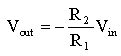 .
.
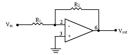
Figure 1: "Inverting amplifier" with 741 op amp.
- Suppose you want to design an inverting amplifier with
gain = -(R2 / R1) = -10.
Ideally, any resistor values that satisfy R2 = 10 R1
will work.
However, with real op amp circuits, the resistor values need to
be chosen with some care.
What would be different in the circuit if R1 = 1 ohm,
R2 = 10 ohm versus R1 = 1 k ohm,
R2 = 10 k ohm?
Look at the data sheet for the
National Semiconductor LM 741 Op Amp, which is available on the Web
at
http://www.national.com/pf/LM/LM741.html
What is the maximum current that the 741 op amp can provide into and out of
its output terminal?
In order to satisfy this limitation, what size resistors should be
chosen for R1 and R2?
- Using the 741 op amp integrated circuit (IC) that will be
provided in lab,
design and set up inverting amplifiers with "gains"
vo / vs = -1, -2, and -10.
For each case, measure the output voltage vo for several
positive and negative input voltages vs.
Are there any limitations to these circuits?
In other words, are there circumstances under which the
desired gain is not achieved?
What is the largest output voltage that your circuit can achieve?
Can you explain why?
You can obtain the pin diagram for the 741 op amp from the
data sheet on the web, or you can refer to Figure 2 below.
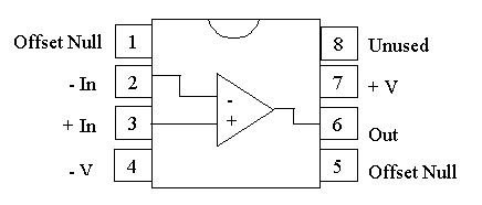
Figure 2: Pin diagram for 741 op amp.
The pin numbers are also indicated in the circuit in
Figure 1 above.
We will use "supply" voltages +V and -V in Figure 2
equal to +12 volts and -12 volts, respectively.
- Suppose you want to design an inverting amplifier with
a variable gain using a potentiometer (pot) whose resistance
varies from a few ohms to 10 k ohms as a dial is turned.
(This might be used for a volume control in a radio.)
Should the pot be placed at R1 or R2?
A microphone, speaker, and pot will be supplied so that you can
demonstrate an amplifier with a variable gain.
Record your circuit designs, measured results, and explanations
in your lab notebook.
3. A Summing Amplifier
Many applications require that two or more signals be added
while also being amplified.
This need arises frequently in audio systems.
For example, in a music performance, we might have several
microphones, each connected to a different singer or instrument.
A "mixing panel" is usually available that allows each
microphone signal to be amplified separately before being
added and sent to the speakers.
An op amp circuit that amplifies and adds signals is shown
in Figure 2.17 on page 77 of the text.
Let us generalize the circuit slightly by replacing the
resistors R1 by different resistors
Ra and Rb connected to the input sources
va and vb, respectively.
- Show that
vo = -(R2 / Ra) va
-(R2 / Rb) vb.
Does this circuit amplify and add two voltages?
- Design an inverting, summing amplifier whose output
voltage is the negative average of the two input voltages.
Record your design in your notebook, and demonstrate the
circuit operation to the lab instructor.
Are there any limitations on the size of the input signals
so that the circuit correctly outputs the negative average?
- Explain how two potentiometers can be used to provide
an "audio mixer" for two microphones with variable gains.
Demonstrate the mixer circuit.
4. Digital-to-Analog Conversion
A digital-to-analog (D/A) conversion circuit is needed in any system
that produces an analog output signal (voltage) based on inputs
that are digital (0's and 1's or binary).
An example that all of us are familiar with is the audio compact
disk (CD).
The music is digitally encoded on the CD, but your CD player
converts the 0's and 1's into an analog music signal that is played
through your speakers.
Let us consider a 3-bit D/A converter.
A binary (base 2) number with 3 bits
b2b1b0
is equivalent to the decimal (base 10) number
22 b2 +
21 b1 + 20 b0
=
4 b2 +
2 b1 + b0.
For example, the binary number 110 is equivalent to the decimal number 6.
Use the summing amplifier studied in the previous section
to design a 3-bit D/A conversion circuit.
Assume that a binary '0' is represented by a 0 volt source,
while a binary '1' is represented by a +5 volt source.
Pages 891-893 in the text discuss D/A conversion.
The circuit in Figure 13.37 will be useful, if you take the
output after the first op amp at v1.
With reference to Figure 13.37, your D/A converter should
operate as follows.
    A2    A1    A0      Output voltage v1
    --    --    --      -----------------

    0V    0V    0V       0 V
    0V    0V   +5V      -1 V
    0V   +5V    0V      -2 V
    0V   +5V   +5V      -3 V
   +5V    0V    0V      -4 V
   +5V    0V   +5V      -5 V
   +5V   +5V    0V      -6 V
   +5V   +5V   +5V      -7 V
Please do the following activities.
- Design the D/A converter, specifying all resistor values
and explaining your reasoning.
- Build the circuit and demonstrate that it operates properly.
- The D/A converter in a CD player must convert 16-bit binary
numbers to analog voltage values.
If you were to extend your design to 16 bits with the
output voltage level between 0 V and -10 V,
which resistor values would be needed in your circuit?
- The D/A converter in Figure 13.38 of the text uses an
R-2R ladder.
Why is this design better than your previous design,
particularly if you extend to 16 bits?
- Do your best to explain the analysis of the R-2R ladder
D/A converter that is presented on page 893 of the text.
Try to explain the analysis to the lab instructor.
The analysis uses the principle of superposition and facts
about combinations of series and parallel resistors.
Include a discussion of the operation of the circuit in your lab notebook.
- Each student should individually design and
construct a 3-bit D/A converter using an R-2R ladder,
as in Figure 13.38.
That is, each student should construct a circuit on their breadboard.
Specify the resistor values in your lab notebook, with an
explanation of your reasoning in choosing the values.
Your circuit should operate according to the following table.
    A2    A1    A0      Output voltage v2
    --    --    --      -----------------

    0V    0V    0V       0 V
    0V    0V   +5V      +1 V
    0V   +5V    0V      +2 V
    0V   +5V   +5V      +3 V
   +5V    0V    0V      +4 V
   +5V    0V   +5V      +5 V
   +5V   +5V    0V      +6 V
   +5V   +5V   +5V      +7 V
For your convenience, the circuit in Figure 13.38
is shown in Figure 3 below, with slightly different notation.
The variables A0, A1, A2,
v1, v2 in Figure 13.38 correspond to
V0, V1, V2,
Vb, Va in Figure 3 below, respectively.
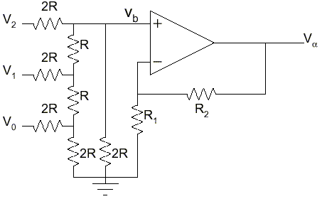
Figure 3: A 3-bit D/A converter using an R-2R ladder.
- On
Thursday, February 15,
** changed to February 22 **
each student will individually
demonstrate his/her circuit.
The purpose of having each student do this individually
is to make sure that all of you are progressing in your EE lab skills.
If you would like, you may wire your circuit before coming to lab
on February 15, and
you may leave lab after demonstrating your circuit.
-
Also on February 15,
** changed to February 22 **
please hand in your lab notebook so that
Labs 1-4 can be graded.
Thank you and have fun!